HKU CFL

Please contact Mr. YIP for CFL Safety Orientation User will need to have a face mask before entering CFL Equipment training schedule/manual can be found on HKU Moodle Door access of DI water system can be applied though MUMS

  The University of Hong Kong

  Central Fabrication Laboratory

Accommodated with top-tier facilities made available to the HKU community and beyond.

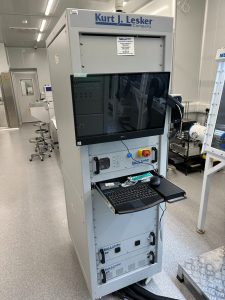
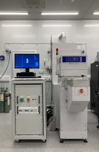
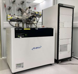
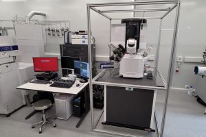
The Central Fabrication Laboratory offers a wide spectrum of fabrication equipment to facilitate different needs in teaching and research.  If you wish to use any specified equipment, please apply for access using the form.
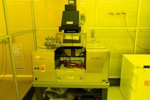
Lithography


MA/BA6 Gen4 (Maskaligner)

  • Substrate size: up to 150mm round wafers
  • TSA alignmTop Side Alignment; ent accuracy: <0.5µm
  • LED lamp house (include I-line, G-line, H-line)
  • MO Exposure Optics
  • Intensity uniformity <2.5%
  • Constant dose accuracy: 1.5%
  • Resolution down to 0.8 µm L/S (vacuum contact)
Maskless

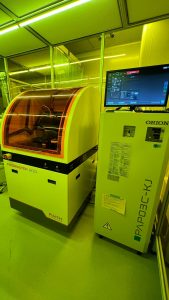
PM200 (Maskless lithography)

  • 375 nm source available for more demanding applications
  • Critical dimension of 300 nm
  • 4 PICO Litho’s proprietary light weight objective lens
  • Supports substrates from 5 x 5 mm2 up to 8”x 8”

Deposition

Mini SPECTROS-Sputtering (PVD-Sputter)

  • Three 3” Torus® Magnetron Sputtering sources
  • DC sputtering power source: 1500 W
  • RF sputtering power source: 300 W at 13.56 MHz
  • Base pressure: 5 x 10⁻⁷ torr
  • Substrate size: 2~6 inch Si/glass substrate, small specimen
  • Substrate fixture: rotation and water cooling
  • Target available: Al, Cu, ITO, Ni, Pt, SiO2 & Ta2O5
  • Deposition rate: SiO2 25 Å/min; Cu 170 Å/min

Mini SPECTROS-E-beam (PVD-E beam)

  • 4 pocket 8 cc Electron Beam Evaporation Source
  • E-beam power source: 5 KW
  • Base pressure: 5 x 10⁻⁷ torr
  • Substrate size: 2~6 inch Si/glass substrate, small specimen
  • Substrate fixture: rotation and water cooling
  • Film thickness controller with 2 crystal sensors
  • Source available:  Al, Au, Cr, Pt & Ti

Mini SPECTROS-Thermal (PVD-Thermal)

  • Three Thermal Evaporation Sources
  • Thermal Evaporation power source: DC power supply, up to 12 V or 400 A, max 2 kW applied power
  • Two 10cc Low Temperature Evaporation organic material sources
  • Two 1cc Low Temperature Evaporation organic material sources
  • Base pressure: 5 x 10⁻⁷ torr
  • Substrate size: 2~6 inch Si/glass substrate, small specimen
  • Substrate fixture: rotation and 350 °C heating
  • Film thickness controller with 3 crystal sensors
  • Source available:  Ag, Al, Au, Cr & Cu

Etching

PlasmaPro 100 Cobra (ICP)

    • Gases available: Ar, CF4, C4F8, O2 & SF6
    • RF Power source: 600 W(max) at 13.56 MHz
    • Electrode coolant system:  -30~80 °C
    • Substrate size: 2~8 inch Si/glass substrate, small specimen
    • Etch rate:

    Silicon Dioxide: 250 A/min

    Silicon Nitride: 190 nm/min

    • Uniformity (within wafer): ± 5%

Ion Beam Etching and Deposition system (IBE)

    • Gases available: Ar, CF4 & O2
    • Power Source: 100 W / 2.45 GHz
    • Sample substrate size: Maximum 4 inch, 3 mm thickness; small specimen
    • Target size: Maximum 3 inch, 3 mm thickness
    • Ion flow stability: ± 5% / 2h (1500 V, High acceleration electrode, Ar gas)
    • Etch rate:

    Si with Fluorocarbons gas: 860 Å/min

    Quartz with Fluorocarbons gas: 1000 Å/min

Helios 5 CX with ELPHY MultiBeam (FIB-EBL)

  • Fastest, easiest and the most automated preparation of high-quality samples for HR S/TEM with AutoTEM 5
  • Access to ultra high-resolution imaging with the most precise contrast for users with any experience
  • Easiest access to high resolution, multi-scale and multi-modal subsurface and 3D information
  • Fastest, most accurate, and precise milling and deposition of complex structures with critical dimensions of less than 10 nm

Diffusion


ALD

ALD-150LE™ (ALD)

  • Purely thermal configuration
  • Substrate size: up to 6” (150 mm)
  • Deposition Uniformity: Thermal Al2O3 ± 1%
  • Typical Processes: Al2O3, HfO2
  • Deposition rate: 0.8 Å/cycle
  •  

Characterization

Sigma 300 VP (SEM)

  • High resolution for both SE and BSE in high vacuum mode
  • VP mode using nitrogen as imaging gas at pressures between 10 and 133 Pa
Profiler

D-600 (Surface Profiler)

  • Vertical resolution: 0.38 Å
  • Lateral resolution: 100 nm
  • Max scan length: 55 mm max.
  • Scan speed:  0.1 ~ 0.4 mm/s
  • Stylus force: 0.03~15 mg
  • Stylus radius: 2 um
  • Display mag.: 1~4 x

VPPA53MET-FL (Microscope)

  • Colour Corrected Infinity Optical System
  • Fluorescence filter sets: AT-EDFP/FiTC/Cy2/AlexaF luor 488; AT-TRITC/Cy3/AlexaFluor 546
  • Objectives: 5 X/0.15 (WD 20 mm); 10 X/0.3 (WD 12 mm); 20 X/0.5 (WO 3 mm); 50 X/0.8 (WD 1 mm); 100 X/0.9 (WD 3.3 mm)
  • Dimension measurement tool 

Others

Direct-Q Deionized Water System

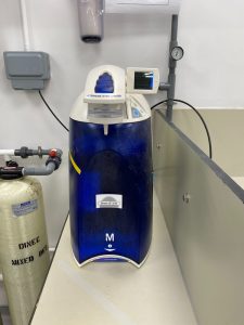
  • This deionized water system can produce about 120L purified water daily which is complied with the ISO 3696:1995 Grade 1 water standard. This systems can remove nearly all ions from your water, including minerals like iron, sodium, sulfate, and copper, which is suitable for laboratory use for the analysis of inorganic chemicals.